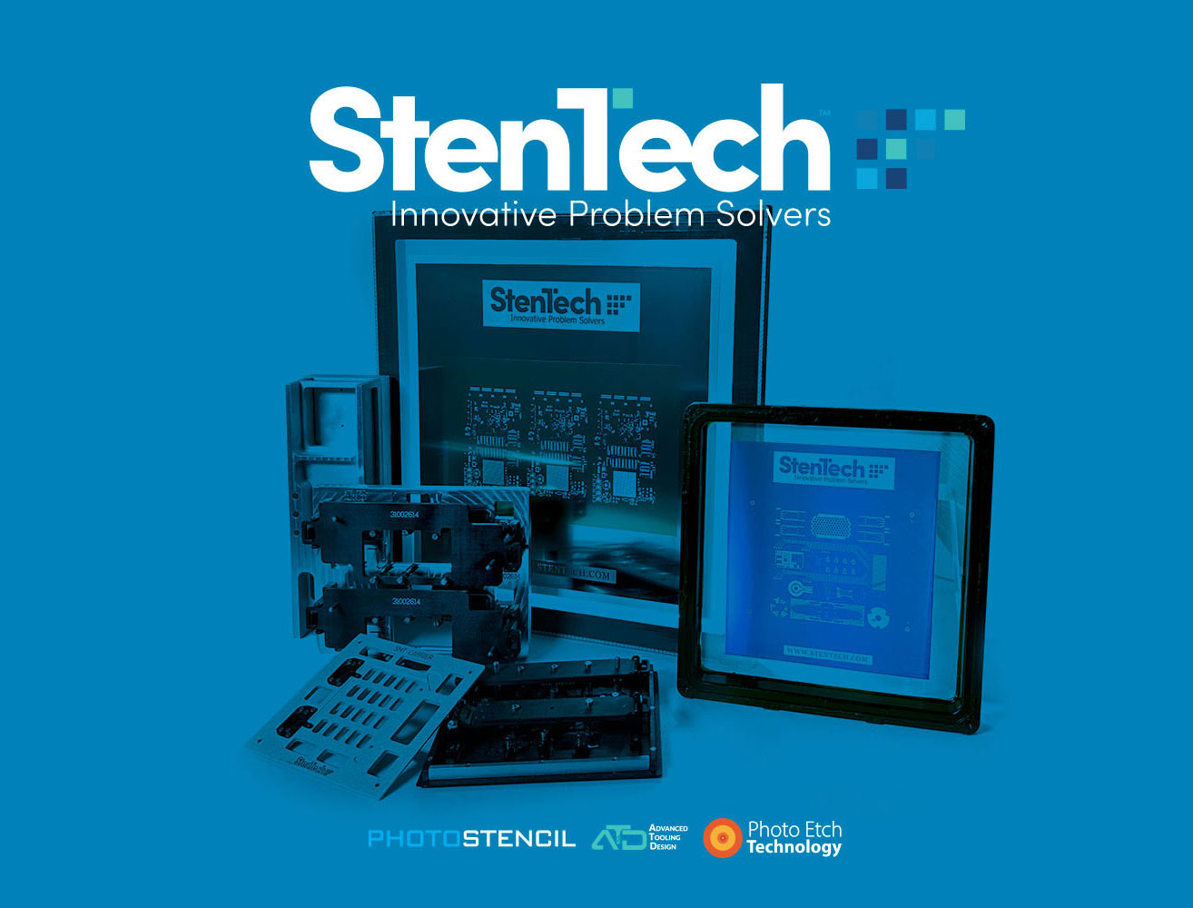
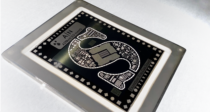
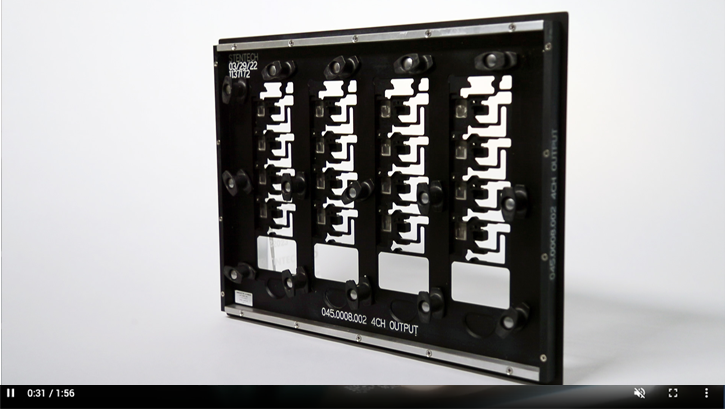
Solder Pallet, Tooling and Parts
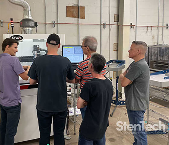
Solder pallet and tooling manufacturing is a crucial aspect of the electronics industry, ensuring precise and efficient assembly processes.
These specialized tools are designed to hold electronic components securely during soldering operations, minimizing errors and enhancing productivity.
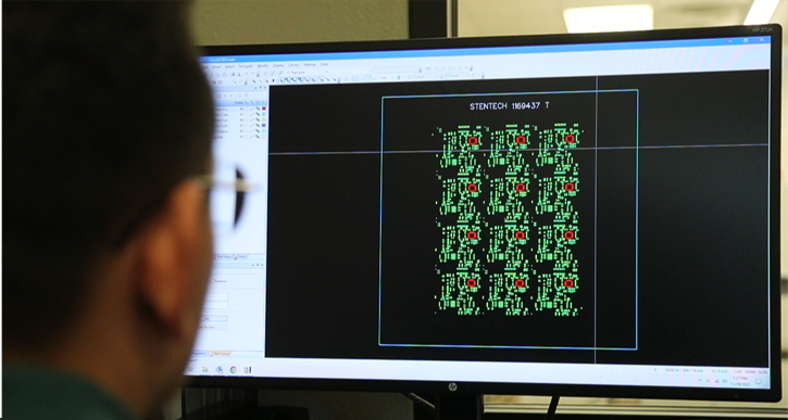
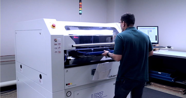
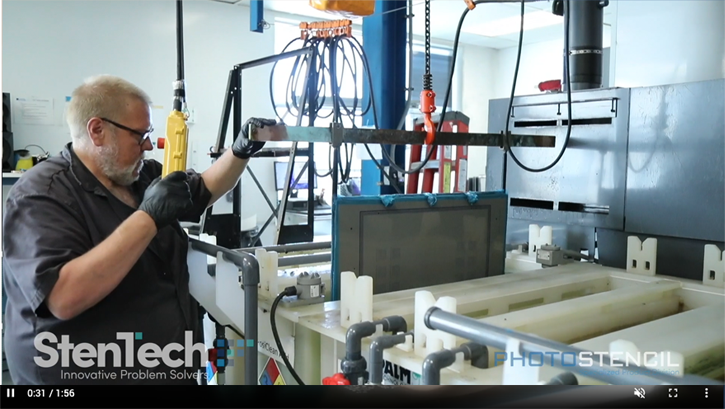
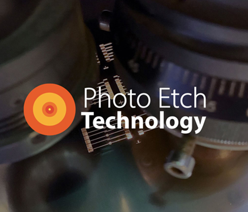
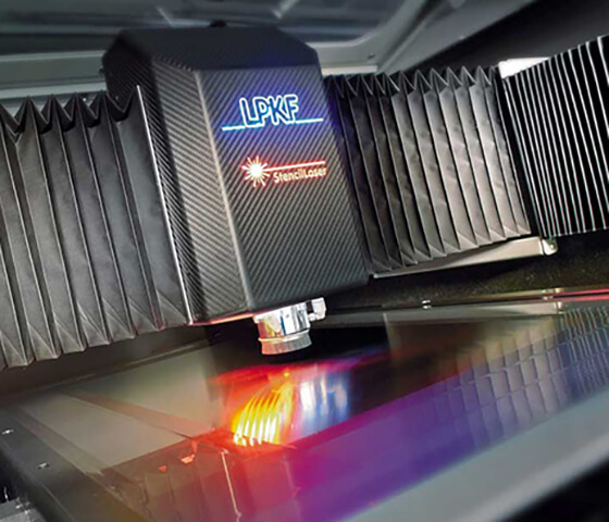
Additionally, chemical and laser etching precision parts play a vital role in creating intricate designs on various materials such as metal or plastic.
This process allows for highly detailed markings or patterns to be etched onto surfaces with utmost accuracy.
Both solder pallet and tooling manufacturing, along with chemical and laser etching, are produced with excellence that meet strict industry standards.
Tooling